Professor Chan Ho Yang of the Department of Physics at KAIST discovered a mechanism behind augmented photoelectric effect when a material bends.
The photoelectric effect converts light energy into electric energy. Because this method can generate electricity without emitting greenhouse gas, research on discovering structures or methods that can efficiently induce the photoelectric effect has been gaining much attention.
Traditional solar devices induce the photoelectric effect by combining other materials or by joining P-N semiconductors. This method is inefficient because it requires two different types of materials and the induced photoelectric effect is not strong enough to be commercially viable.
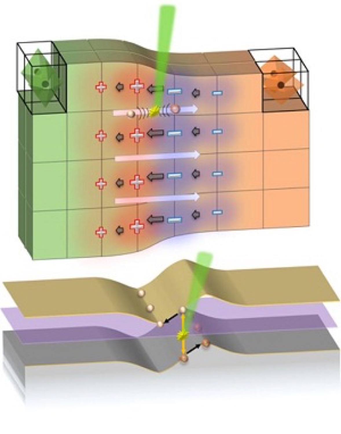
However, Professor Yang's research team discovered that the bending of a single material showed a phenomenon similar to that of the photoelectric effect seen on the boundary of two different materials. Thus, the team corroborated that an electric field can be created not only by joining P-N semiconductors but also by flexing a single material. Regular bending of a material did not induce significant photoelectric effect, thereby lacking efficiency. However, the research team observed structures on the nano-scale and discovered a range in which a material bends itself to exhibit significant photoelectric effect.
Furthermore, the research team confirmed that the bending on the nanometer scale produces an electric field 100 times stronger than that of other regular materials. The reason lies in the electric field which is produced upon the flexion of the material. When a material receives light, electrons bound to the atom can move for a while but they usually become bounded again. However, in the range that the research team unveiled, electric field is created in a significant level, allowing electrons to escape from the atom to create a current.
This research is expected to be widely applicable because structures in the nanometer scale often exist in a largely bent manner. Moreover, the research team developed a technology that images electromechanical properties of the surface of a material on a 10 nanometer resolution. This allows researchers to infer the distribution of electrical fields, which can be applied to various nano-scale researches. Furthermore, this research can be applied to various fields such as info-communications, data storage, and photoelectric sensors. This research was published on Nature Nanotechnology on August 31.